Tutorial 1: RFSoC Platform Yellow Block and Simulink Overview
In this tutorial, you will make a simple design for an rfsoc board using the
CASPER toolflow. It will take you through launching the toolflow, creating a
valid CASPER design in Simulink, generating an .fpg and .dtbo file,
programming the .fpg and .dtbo file to a CASPER rfsoc board, and interacting
with the hardware running on the board using the casperfpga library through a
python interface.
This tutorial assumes that you have already setup your environment correctly, as explained in the Getting Started With RFSoC tutorial, specifically that the correct versions of Vivado and Matlab are installed. You should also have all the programs and packages installed, configuration files set, and have successfully set up and tested your connection to the rfsoc board.
Creating Your First Design
Create a New Model
Make sure you are in your previously set up environment and navigate to
mlib_devel. Start Matlab by exectuing startsg. This will properly load
the Xilinx and CASPER libraries into Simulink, so long as your startsg.local
file is set correctly. Within Matlab, start Simulink by typing simulink into
Matlab’s command line. Create a new blank model and save it with an appropriate
name. The name cannot contain capital letters. If you use capital letters your
design will not compile correctly.
There are also premade starter simulink designs that can help you get started. You can find
them in the tut_platform folder here.
Library Organization
There are three primary libraries in Simulink you will use when designing for your rfsoc board:
- The CASPER XPS Library contains the CASPER “Yellow Blocks”. These blocks encapsulate interfaces to your board’s hardware (ADCs, memory chips, CPUs, various ports, etc).
- The CASPER DSP Library contains (often green) blocks that implement DSP functions (filters, FFTs, etc).
- The Xilinx Library contains blue blocks which provide low-level fpga
functionality (multiplexing, delaying, adding, etc). It also contains the
System Generatorblock, which contains information about the FPGA you are using.
Add the Xilinx System Generator and CASPER Platform blocks
The first thing to add is the System Generator block, found using the Simulink
Library Browser in Xilinx Blockset->Basic Elements->System Generator. Add the
block by clicking and dragging the block into your design. See the Simulink
documentation by Mathworks for other methods of finding and adding blocks to
your design.
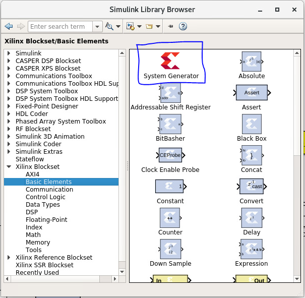
You can double-click on the added block to see its configuration. However,
instead of configuring the System Generator ourselves, we will use a platform
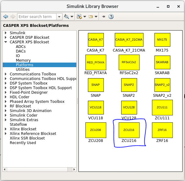
Yellow Block from the CASPER XPS Library to configure it. Locate the block
for the board you are using in CASPER XPS Blockset->Platforms-><your
platform>. This example uses the ZCU216 pltform block, so this example adds
the ZCU216 Yellow Block to our Simulink model. All RFSoC platfrom Yellow Blocks
are similar in their configuration. The following is therefore easily applied to
your specific platform.
Note: The System Generator and XPS platform blocks are required by all CASPER designs
Double-click on the added platform block to see its configuration.
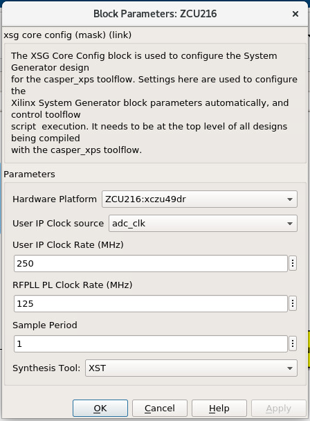
Confirm that the Hardware Platform parameter matches the platform you are
using. The User IP Clock Rate is the desired frequency for the IP of the
design. For the RFSoC platform the adc_clk user IP clock source is derived
from the pl_clk coming from the first stage PLL in the clocking hierarchy for
the RFDC. In most cases this is an LMK creating the pl_clk in addition to the
clock that drives the RFDC tiles. This frequency coming from the LMK as pl_clk
is what is to be entered into the RFPLL PL Clock Rate field. In other words,
this is the clock rate the design is expecting to produce the clock frequency
for the user IP clock.
Before proceeding briefly review the clocking information for your target platform and any additional setup/configuration required:
Set the User IP Clock Rate and RFPLL PL Clock Rate as follows for your
target RFSoC platform:
# ZCU216
User IP Clock Rate: 250, RFPLL PL Clock Rate: 125

# ZCU208
User IP Clock Rate: 250, RFPLL PL Clock Rate: 125

# ZCU111
User IP Clock Rate: 245.76, RFPLL PL Clock Rate: 122.88

# RFSoC 4x2
User IP Clock Rate: 245.76, RFPLL PL Clock Rate: 122.88

# RFSoC 2x2
User IP Clock Rate: 245.76, RFPLL PL Clock Rate: 15.36

# ZFR16
User IP Clock Rate: 250, RFPLL PL Clock Rate: 50
The Example Design
In order to demonstrate the basic use of hardware interfaces and software interaction, this design will implement three different functions on the board:
- A Flashing LED
- A Software Controllable Counter
- A Software Controllable Adder
The final design will look something like this:
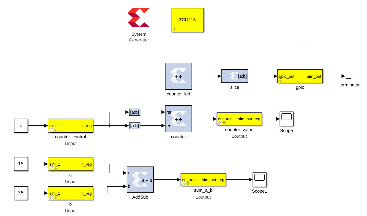
Function 1: Flashing LED
We can create a flashing LED by using a 27-bit counter. On the ZCU216, the default clock given by its CASPER platform block is 250 MHz, which will toggle the most significant bit on the 27 bit counter about every 0.27 seconds. The principle is the same for any clock rate on any board. We can output this most significant bit to an LED on the board, causing the LED to flash at about 50% duty cycle every so many seconds (half a second for this example).
Step 1: Add a counter
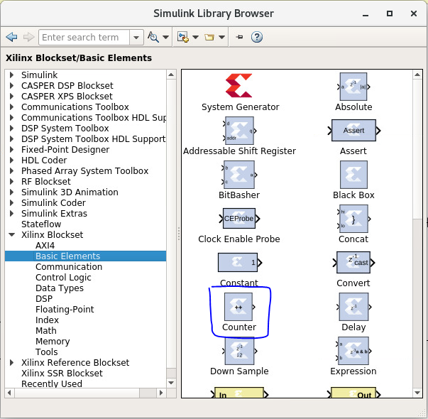
Add a blue counter block to the design. It can be found in Xilinx
Blockset->Basic Elements->Counter.
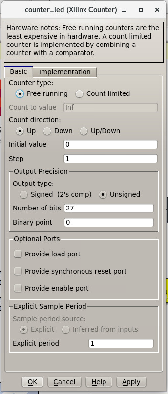
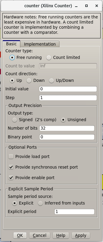
Double-click the block to access its parameters, and set it to free running,
27-bits, unsigned. This will set the counter to count from 0 to (2^27)-1,
wrap back to zero, and continue.
Step 2: Add a slice block to select the MSB
Now that we have a counter, we want to select just the most significant bit so
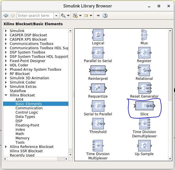
that we can send it to an LED. Do this by adding a blue slice block, found in
Xilinx BLockset->Basic Elements->Slice.
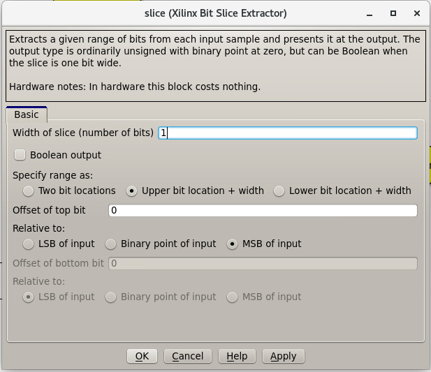
Double-click on the slice block to modify it. There are several ways to use the slice block to grab the bit we want. For this example, we will select the MSB by indexing from the upper end and selecting the first bit.
Step 3: Add a GPIO Block
Next we want to access an LED to send that bit to. We can access the correct
FPGA output pin by using a GPIO block. GPIO blocks allow you to route signals
from Simulink to various FPGA pins. Add a yellow GPIO block, found in CASPER
XPS Library->IO->gpio.
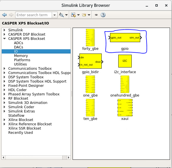
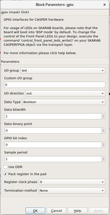
Double-click the gpio block and set it to the led I/O group. Set the I/O
direction to out, the data type to boolean, the data bitwidth to 1, and
the GPIO bit index to 0. This tells the toolflow that it will be connecting
a 1-bit input to LED0.
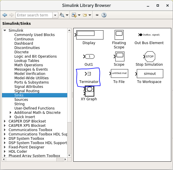
Step 4: Add a terminator
To prevent warnings (from MATLAB & Simulink) about unconnected outputs,
terminate all unused outputs using a Terminator block.
Step 5: Connect the design
If you haven’t done so already, rename the blocks to sensible names, such as
counter_led instead of counter. You can do this by double-clicking the name on
the blocks.
Connect the blocks together by clicking and dragging from the output arrow on one block and dragging it to the input arrow on another block.
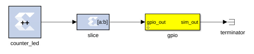
And you’re done with the flashing LED!
Function 2: Software Controllable counter
Next we will design a hardware counter that we can start, stop, reset, and read using software. The design will look similar to the flashing LED we just finished.
Step 1: Add the software registers
In order to interact with the hardware while it’s running, we need some software
registers. For our counter, we want two software registers, one to control the
counter, and another to read it’s current value. Add two yellow
software_register blocks to the design, found in CASPER XPS
Blockset->Memory->software_register.
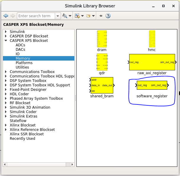
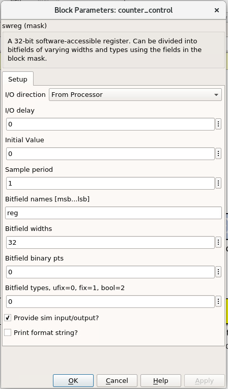
On one of the software_register blocks, set the I/O direction to From
Processor. This will allow a value from the software to be sent to the FPGA
hardware. This block will be the counter controller.
On the other software_register block, set the I/O direction to To Processor.
This will allow the FPGA hardware to send a value to the software when prompted.
This block will be what allows us to read the counter.
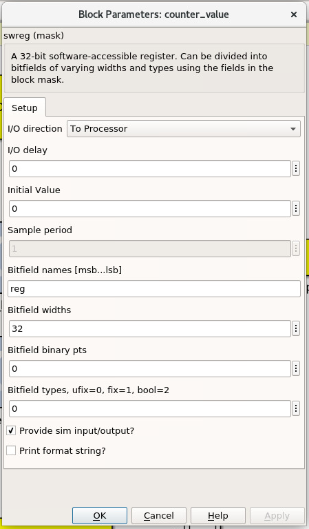
Set both registers to a bitwidth of 32-bits and rename them something sensible.
The names of the blocks here are the names used to access them from
casperfpga. Do not use spaces, slashes, or other funny characters for these
names. In this example, they are named counter_control and counter_value.
See that the registers have sim inputs and outputs. These allow you access the
blocks in Simulink for simulation and test purposes. A sim input port can be
fed inputs by simulink blocks, and a sim output port can be read by simulink
blocks.
So that the counter runs during simulation, add a simulink constant block (found
in Simulink->Sources->Constant), set it to 1, and connect it to the ‘sim’
input of the counter controller register. To monitor the counter’s value in
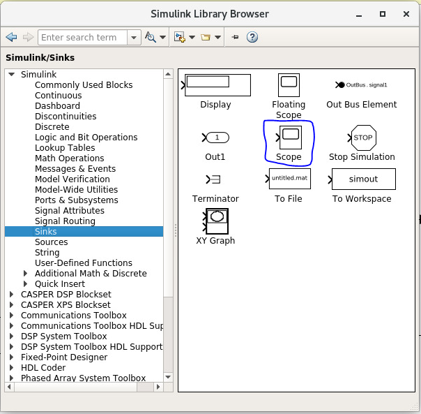
simulation, add a simulink scope block (found in Simulink->Sinks->Scope) and
connect it to the sim output of the counter value register.
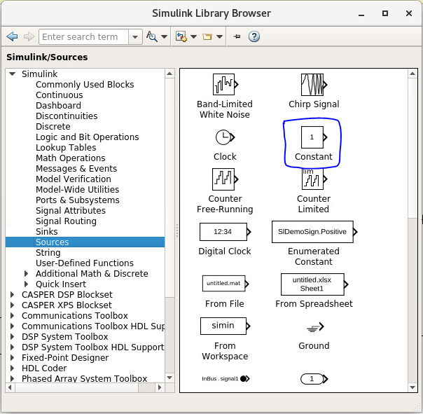
Note that these white simulink blocks will not be compiled to the fpga hardware. They are for simulation purposes only. Only blue System Generator blocks are acutally compiled. Yellow blocks are required to interface white simulink blocks to the blue System Generator blocks.
Step 2: Add the counter
Add another counter block the same way we did before. You can also copy the existing counter block by the usual copy-paste or by ctrl-click-drag-drop. Open it’s paramters and set it to free running, unsigned, 32-bits, with synchronous reset port and enable port turned on.
Step 3: Add the slice blocks
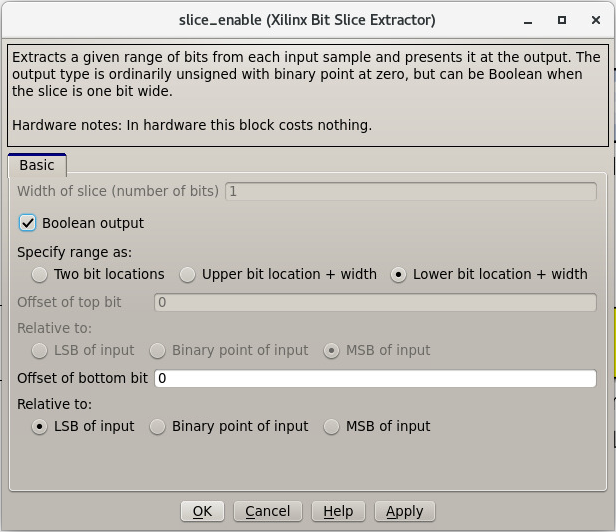
We want to be able to control the enable and reset ports on this new counter with the counter control register we made before. We can do this by slicing out one bit of the register for the enable port and slicing out another bit for the reset port. Alternatively, we could use two seperate registers, one for the reset and one for the enable, but as the registers are 32-bits each, that would be wasteful.
Add two new slice blocks (or copy them from the flashing LED function). Configure
one slice block for the enable by setting it to boolean output, specifying the
range as Lower bit location + width, offset 0, and relative to LSB of
input.
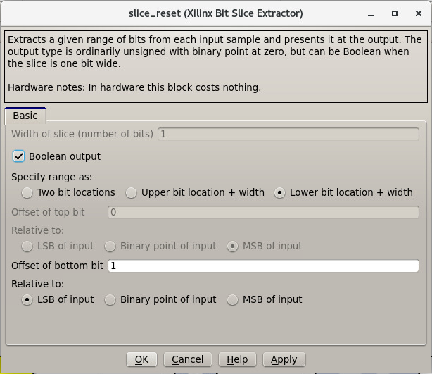
Configure the other slice block for the reset with the same approach, but
setting the offset to 1.
Step 4: Connect the design
Connect the blocks together. Take time to make the design look neat as well, renaming and resizing blocks as needed.
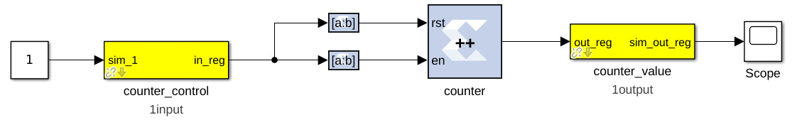
And that concludes this counter!
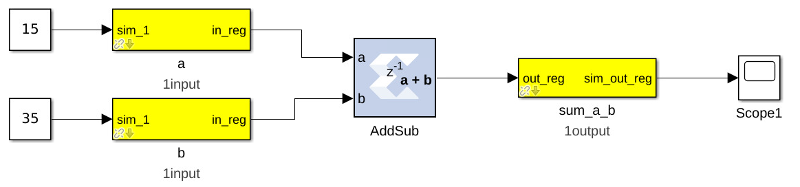
Function 3: Software Controllable Adder
The last function we will implement is a software controllable adder. We will be able to give the adder two value over software, it will add in the hardware, and we will be able to read the result back using software.
Step 1: Add the software registers
Add two software registers and configure them as inputs (From Processor).
These will let us specify the values to add. Add another register and configure
it as an output (To Processor), so that we can read back the result. Name
them something reasonable. Remember that the register names are how they will be
accessed by the software.
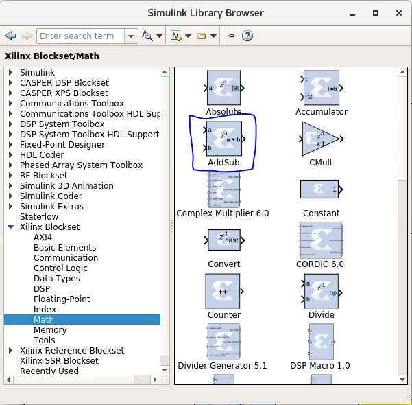
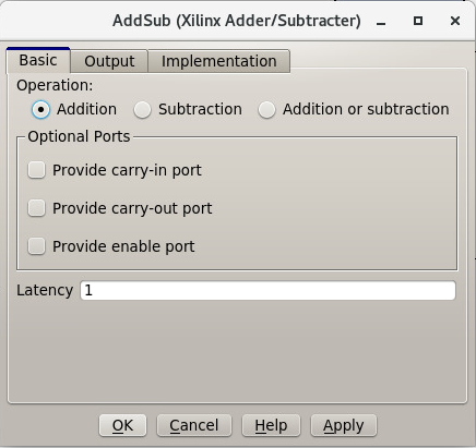
Step 2: Add the adder block
Add a blue adder/subtractor block to the design, found in Xilinx
Blockset->Math->AddSub. Check its configuration and make sure it is set to
addition.
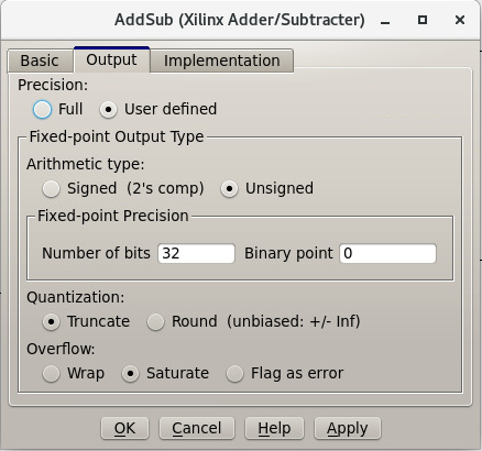
The output register is 32-bits. If we add two 32-bit numbers, we will have 33-bits.
There are a number of ways of fixing this:
- limit the input bitwidth(s) with slice blocks
- limit the output bitwidth with slice blocks
- create a 32-bit adder.
For this example, we will configure the AddSub block to be a 32-bit adder. In
its configuration, under the Output tab, set it to unsigned 32-bits. Also set
its overflow to Saturate. This way if two very large numbers are added, it will
just return its max (2^32-1).
Step 3: Add the scope and simulation inputs
Add simulink scope and constant blocks to the output register and input registers. Set the constant blocks to something so we can check the adder in simulation.
Step 4: Connect the design
Connect all the blocks together, name things properly, and adjust/resize the design so it is easy to look at. Of course, these can all be done as you go, and probably should be done as you go.
Now the adder is done!
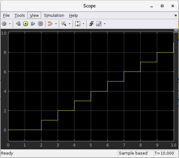
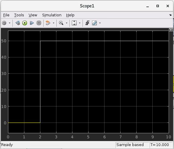
Simulating the design
With all hardware functions configureed has hooked up, we can simulate the design with Simulink.
Under the simulate section of the simulation tab on the ribbon, set the stop
time to the number of clock cycles you want to simulate. This example uses
10. Note that (at least in MATLAB R2020b) it says that the stop time is in
seconds, but this is actually clock cycles because of the way the toolflow and
CASPER blocks are configured.
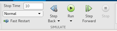
Press Run to simulate the design. Once the simulation is done, and assuming
there are no errors, you can double-click the scopes to view the output signals.
You should see the counter incrementing once every clock cycle and the adder
should show you the result of the addition. You may have to scale the scopes to
see the results properly.
Once everything looks like it should, you’re ready to compile for the FPGA!
Compiling
We now have a design with three independent functions all working off the same FPGA clock. From here, compiling the design is easy, so long as your environment was set up correctly.
To compile the design, go to the MATLAB command line and enter
>> jasper
Depending on your computing resources compilation of this design will take between 10 and 25 mins.
The jasper command will run the various parts of the build process. The first
part uses Xilinx’s System Generator to compile any Xilinx blocks in the design
to a circuit that can be implemented on the FPGA, i.e., HDL code.
The second part runs Vivado’s synthesis, implementation and place and route
tools creating the physical hardware design for the FPGA. Lastly, the toolflow
creates the final output .fpg and .dtbo files that are used to program the
FPGA using CASPER software framework. The .fpg file contains the bitstream
that Vivado created as well as meta-data that describes the yellow blocks from
the simulink design and their configurations. The .dtbo is a new output
product of the toolflow targeting SoC platforms like the RFSoC.
Similar to the meta-data that is created for CASPER softawre the .dtbo is the
device tree overlay binary containing somewhat similar meta data information but
taragetd to the software drivers that will be loaded by the processor system
when programming the FPGA. After Vivado syntheis and bitstream generation the
toolflow exports the platform hardware definition to use Xilinx’s software tools
(the Vitis flow) to generate software produts to interface with the hardware
design. The .dtbo is one of those software products. The .dtbo is now used
in conjunction with the .fpg file where the .fpg is used to first program
the FPGA followed by application of the device tree overlay. In this design
there are no IP that take advantage of this and so the resulting .dtbo will be
mostly empty (the MPSoC is always present in the design). Both the .fpg and
.dtbo file will be placed in the outputs folder in the working directory of
the Simulink model. The files will be named using the simulink file name and the
date/time that compilation began.
Note that the .dtbo must be placed in the same directory as the .fpg and
have the same name (except for the extension). Meaning if the .fgp file name
is changed from the compiled default, the .dtbo must also be updated as well.
Programming the FPGA
Reconfiguration on any CASPER platform is typically done using the casperfpga
python library. However, before we use casperfpga we are going to instead
manually connect to the board to program the clocks needed for the user design.
This is done to briefly introduce the processing system and idea that as a user
the processor is there to be used if needed.
Programming the onboard clocks for the RFSoC can be done using the rfdc yellow
block and associated RFDC casperfpga object (to be introduced in the next
tutorial). However this does not use the rfdc yellow block meaning an RFDC
object is not automatically present on the software side. There are other ways
to program these clocks using casperfpga but instead we can also use a basic
software utility that is distributed with each platform to do this.
shell into the board using an ssh client, the default username is
casper with password casper. For example,
$ ssh casper@your.ip.address.here
In the home directory there is a bin directory containing a few utilities for
some of the board on-board peripherals. Specifically, each platform will have a
utility to program the PLLs that are to drive the sample clock or PLL for the
RFDC. Take a look at that directory, it is shown here for all the platforms.
casper@alpaca-1:~$ ls bin/
prg_8a34001  prg_clk104_rfpll  reset_rfpll  zcu216_probe_sfp
The program to configure the LMK/LMX PLLs for the RFDC all accept a .txt
formatted hexdump file from TICS with the commandline switch -lmk or -lmx
to indicate the target PLL.
casper@alpaca-1:~$ ./bin/prg_clk104_rfpll
must specify -lmk|-lmx
./bin/prg_clk104_rfpll -lmk|-lmx <path/to/clk/file.txt>
The distributed clock files for the platform are stored in /lib/firmare. As
mentioned above,
designs for RFSoC use pl_clk coming from the on board LMK to generate the User
IP clock. Program the LMK using the corresponding platforms utility (before
proceeding make sure to have reviewed your platforms page
for required clocking configuration and setup):
# ZCU216
casper@alpaca-1:~$ sudo ./bin/prg_clk104_rfpll -lmk /lib/firmware/250M_PL_125M_SYSREF_10M.txt

# ZCU111
casper@alpaca-zcu111:~$ sudo ./bin/prg_rfpll -lmk /lib/firmware/122M88_PL_122M88_SYSREF_7M68_clk5_12M8.txt

# RFSoC 4x2
casper@rfsoc4x2:~$ sudo ./bin/prg_rfpll -lmk /lib/firmware/rfsoc4x2_PL_122M88_REF_245M76.txt

# RFSoC 2x2
casper@rfsoc2x2:~$ sudo ./bin/prg_rfpll -lmk /lib/firmware/rfsoc2x2_lmk04832_12M288_PL_15M36_OUT_122M88_CLK12_15M36.txt

# ZRF16
casper@htg-zrf16:~$ sudo ./bin/prg_rfpll -lmk /lib/firmware/zrf16_LMK_CLK1REF_10M_LMXREF_50M_PL_OUT_50M_nosysref.txt
Each platform has an LED connected to the status pin of the LMK that should now be lit indicating that PLL is locked.
The LMXs could also be programmed in the same way using the -lmx switch and a
corresponding LMX hexdump file but this is not needed here as those drive the
sample clock or internal PLL reference clock for the RFDC.
With the clock to drive the user design configured we can now continue to use
casperfpga to program the FPGA and interact with our design. You should have
installed and used this in the Getting Started
tutorial to check your connection to your board.
Step 1: Copy the .fpg file to where you need it
Navigate to the prevously mention ‘outputs’ folder and copy the .fpg file to
wherever you are going to be running your ipython session from.
Step 2: Connect to the board
Assuming that your board is on, configured, and on the same network you are working on, connect to the board the same way demonstrated in the Getting Started tutorial:
$ ipython
In [1]: import casperfpga

In [2]: fpga = casperfpga.CasperFpga('ipaddress.of.board')

In [3]: fpga.is_connected()
Out[3]: True
If the output of is_connect() is true, you’re good to go.
We can now program the fpga with the .fpg file with the following:
In [4]: fpga.upload_to_ram_and_program('/path/to/your_fpgfile.fpg')
Interacting with the board
The design we created is now running on the board! You should see the first
function working by observing the blinking LED on the board. From here we can
check to see if the software registers in the design worked. If you forgot what
the registers were named, you can use listdev() to get a list of available
registers:
In [5]: fpga.listdev()
Out[5]:
['a',
 'b',
 'counter_control',
 'counter_value',
 'sum_a_b',
 'sys_block',
 'sys_board_id',
 'sys_clkcounter',
 'sys_rev',
 'sys_rev_rcs',
 'sys_scratchpad']
Let’s test the adder function first. Reading and writing to the registers can be
done with write_int() and read_int():
In [6]: fpga.write_int('a',15)

In [7]: fpga.write_int('b',35)

In [8]: fpga.read_int('sum_a_b')
Out[8]: 50
Lastly, let’s test the controllable counter:
In [9]: fpga.read_uint('counter_value')
Out[9]: 0

In [10]: fpga.write_int('counter_control',1)

In [11]: fpga.read_uint('counter_value')
Out[11]: 1103388123

In [12]: fpga.read_uint('counter_value')
Out[12]: 1849175237

In [13]: fpga.read_uint('counter_value')
Out[13]: 2590065552

In [14]: fpga.write_int('counter_control',0)

In [15]: fpga.read_uint('counter_value')
Out[15]: 1159837158

In [16]: fpga.read_uint('counter_value')
Out[16]: 1159837158

In [17]: fpga.write_int('counter_control',2)

In [18]: fpga.read_uint('counter_value')
Out[18]: 0
We can see that the counter starts at 0 and does not start counting until it
receives the proper signal in the proper register. We can also see that the
counter wraps properly, and stops and resets as expected according the signals
and registers we designed. Note that read_uint() is used here to read the
counter properly (otherwise it would have reported a negative value half the
time).
Conclusion
In this tutorial, you have gone through the process of using startsg to
initiate the toolflow, used Simulink to create a design, called jasper to
compile and obtain a .fpg and .dtbo file, and use casperfpga to program
and interact with your rfsoc board. Congratulations!