CASPER RFSoC README
Introduction
This documentation aims to introduce Xilinx Zynq UltraScale+ RFSoC to the CASPER community along with the platforms and capabilities currently supported in the CASPER tools. The hardware and design flexibility of RFSoC within CASPER will continue to proliferate the design philosophy of CASPER of decreasing the time-to-science metric and provide a way of bringing the needed capabilities to next generation instruments.
Before starting with the tutorials and reviewing the available platforms, the following is a brief introduction and overview of the RFSoC architecture and its capabilities. The primary source of the information presented here is Xilinx documentation and data sheets pertaining to the Zynq UltraScale+ RFSoC. Please reference those materials (PG269, DS889, and DS926) for more details as this is a rehashing of only some high-level details.
The RFSoC
A high-level block diagram of the RFSoC package is shown in the below figure.
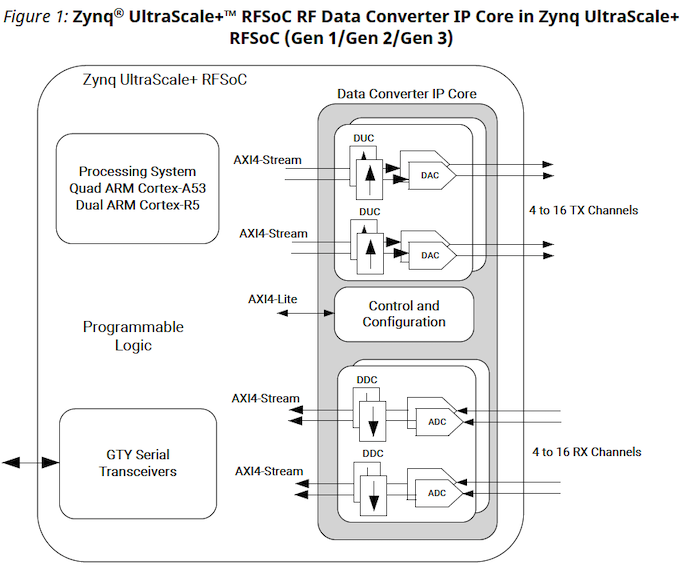
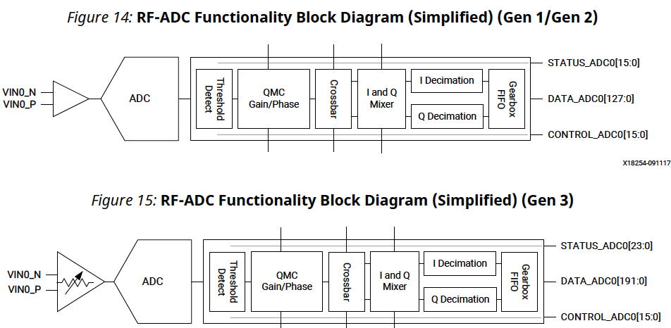
The RFSoC integrates programmable logic with the Zynq ARM (A53) processor, high speed serial transceivers, and the RF Data Converters (RFDC); a hardened IP core implementing all RF functionality. The RFDC groups together multi-gigasample per second ADCs (DACs) capable of direct sampling (synthesis) for RF signals up to 6 GHz (9.85 GHz). Additionally, these cores include digital down (up) converters, a mixer capable of a fixed coarse setting or fine frequency tuning by a numerically controlled oscillator (NCO), and interpolation and decimation filters. A block diagram of the analog signal path for the ADCs is shown in the following figure.
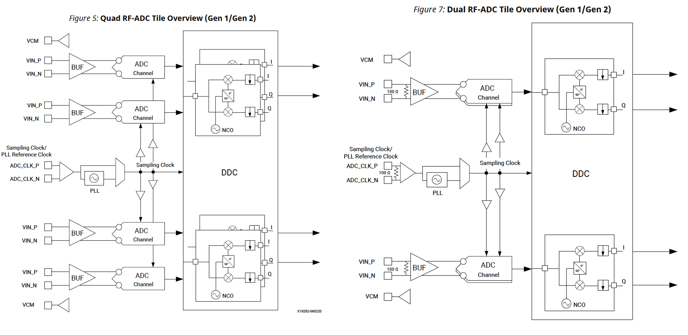
The ADCs and DACs are grouped into “tiles” to some extent similar to the idea of other columnar tile components of a Xilinx FPGA. In this case however, the ADCs or DACs and their supporting components populate the entire tile. There are two different tile architectures found in RFSoC devices: quad-tile and dual-tile. The number of tiles found in the device and their capabilities varies between RFSoC packages and generation. The quad- and dual-tile architectures are depicted in the below figure.
As the RFDC is the focus of the RFSoC, in order to bring the functionality to CASPER an RFDC yellow block is needed to access and configure the IP. This yellow block instances the underlying Vivado RFDC IP and interfaces to the CASPER user in a similar fashion as would be presented to the hardware designer in Vivado providing many of the same configuration options. This was done to maintain the flexibility of the RFDC and provide as much control as possible over its configuration and provide that to the general CASPER user.
The RFDC yellow block is designed to detect the tile architecture (quad/dual) and the generation (gen 1/3) of the selected platform as specified by an RFSoC platform yellow block. This provides a forward compatibility mechanism as more RFSoC platforms are targeted in CASPER and as Xilinx inevitably produces future generations of the RFSoC.
Platforms
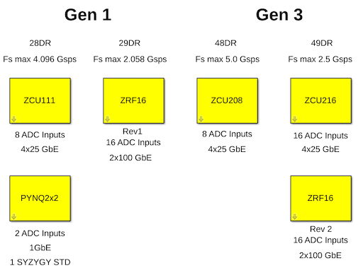
The CASPER library contains support and has been tested for the following RFSoC platforms:
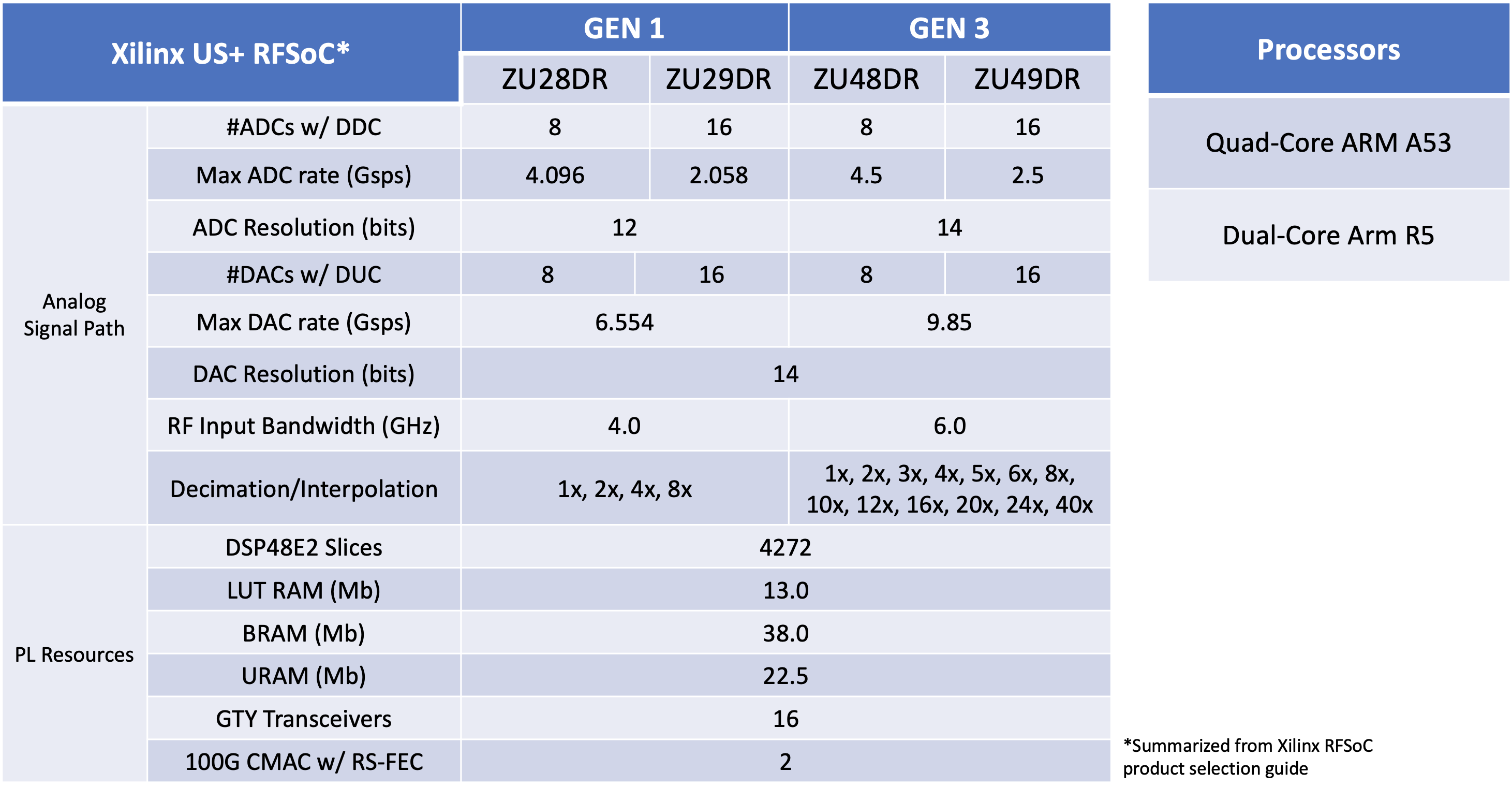
A summary of the board resources taken from the Xlinx RFSoC product selection guide is shown in the following table. In the context of astronomy signal processing these features are ideal for small form factor and low power digitizers streaming raw voltages over 2x100GbE, or suitable as modest sized channelizers using the available fabric resources.