Tutorial 2: The RFDC Interface
Introduction
In this tutorial we introduce the RFDC Yellow Block and its configuration
interface for dual- and quad-tile RFSoCs with a simple design that captures ADC
samples and places them in a BRAM. Software control of the RFDC through
casperfgpa is also demonstrated with captured samples read back and briefly
analyzed. This tutorial assumes you have already set up your CASPER development
environment as described in the Getting Started
tutorial and are familiar with the fundamentals of starting a CASPER design and
communicating with your RFSoC board using casperfpga from the previous
tutorial.
The Example Design
In this example we will configure the RFDC for a dual- and quad-tile RFSoC to sample RF signals over a bandwidth centered at 1500 MHz. There are a few different ways this could be accomplished which vary between the two different tile architectures of the RFSoC on these platforms. In this tutorial, though, we target configuration settings that are as common as possible by using a number of the various RFDC features, while still pointing out some of the differences between the quad- and dual- tile architectures of the RFSoC. When platform specific settings are required beyond what is needed generally, they will be noted.
- This design will:
- Set sample rates appropriate for the different architectures
- Use the internal PLLs to generate the sample clock
- Output complex basebanded I/Q samples
- Use the decimator
- Use the fine frequency mixer (NCO)
- Set the target Nyquist zone
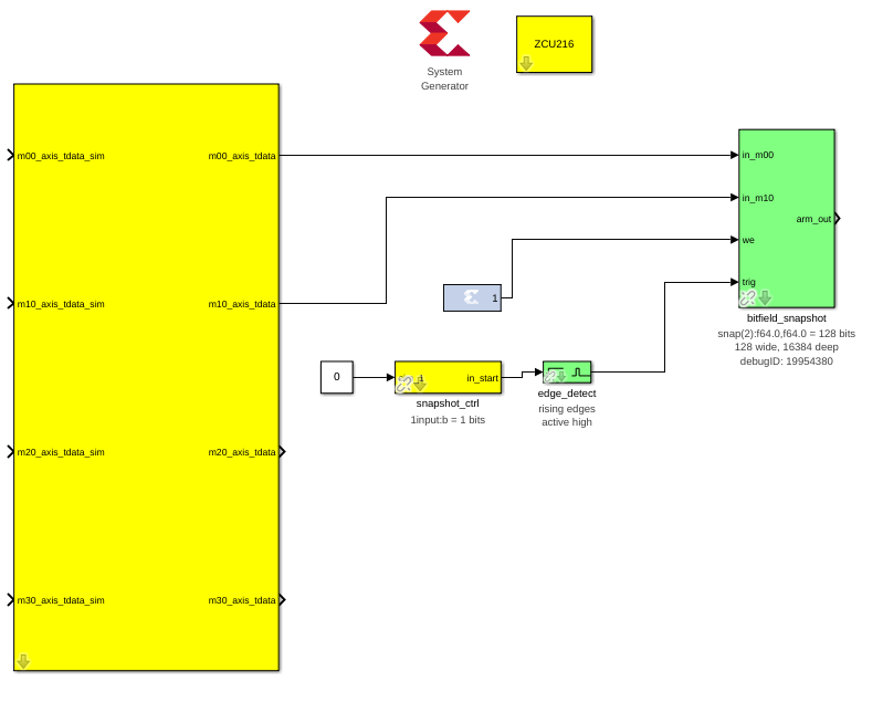
To get a picture of where we are headed, the final design will look like this for quad-tile platforms:
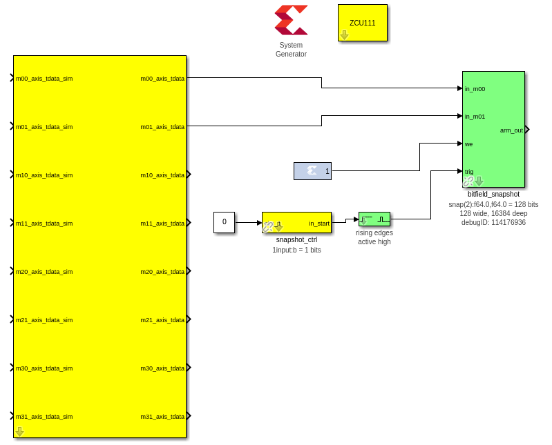
And this for dual-tile platforms:
This design is a “snapshot” capture on two inputs on quad-tile platforms and one
input on dual-tile platforms placing raw ADC samples in a BRAM that are read out
using casperfpga for analysis. The design could easily be extended with more
snapshot blocks to capture outputs from the remaining ports, but what is shown
here is sufficient for the scope of this tutorial.
Step 1: Add the XSG and RFSoC platform yellow block
Add a Xilinx System Generator block and a platform yellow block to the design,
as demonstrated in tutorial 1. While the above example
layouts used the RFSoC 4x2 as the example for a dual-tile RFSoC and the ZCU216
as the example for a quad-tile platform, the steps for a design targeting the
other RFSoC platforms are similar for their respective tile architecture.
Configure the User IP Clock Rate and PL Clock Rate for your platform as:
# RFSoC 2x2
User IP Clock Rate: 245.76, RFPLL PL Clock Rate: 15.36

# RFSoC 4x2
User IP Clock Rate: 245.76, RFPLL PL Clock Rate: 122.88

# ZCU111
User IP Clock Rate: 245.76, RFPLL PL Clock Rate: 122.88

# ZCU208
User IP Clock Rate: 250, RFPLL PL Clock Rate: 125

# ZCU216
User IP Clock Rate: 250, RFPLL PL Clock Rate: 125

# ZFR16
User IP Clock Rate: 250, RFPLL PL Clock Rate: 50
Step 2: Place and configure the RFDC yellow block
Add an rfdc yellow block, found in CASPER XPS Blockset->ADCs->rfdc.
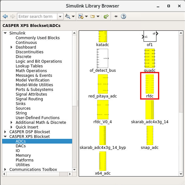
The rfdc yellow block automatically understands the target RFSoC part and
derives the corresponding tile architecture, subsequently rendering the correct
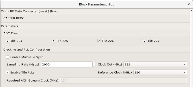
configuration view. For both architectures the first half of the configuration view is
identical. This is the portion of the configuration that sets the enabled tiles,
sample rate, use of internal PLLs, inclusion of multi-tile synchronization
infrastructure, and displays tile clocking information.
For a quad-tile platform configure this section as:
For a dual-tile platform configure this section as:
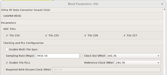
The Enable Tile checkboxes under each Tile tab will enable or disable the corresponding tile in the
design. The tile numbers are in reference to their respective package placement
designation. Tile 224 through 227 maps to Tile 0 through 3, respectively. The
rfdc yellow block will redraw after applying changes when a tile is selected.
The sample rate for each architecture is automatically checked against the min.
and max. sample rates supported for the platform. The Enable Tile PLLs
checkbox will enable the internal PLL for all selected tiles. When this option
is enabled the Reference Clock drop down provides a list of frequencies
that can be used to drive the PLLs to generate the sample clock for the ADCs. If
Enable Tile PLLs is not checked, this will display the same value as the
Sampling Rate field indicating the part is expecting an external sample clock
to drive the ADCs.
- A few behaviors to keep in mind:
- The
Required AXI4-Stream Clockfield indicates what theUser IP Clock Rateof the platform yellow block must be set. There is a DRC within the toolflow that checks to make sure the values match. However, this does require that the CASPER designer make sure the two fields remain in sync. - The RFDC IP has an optional
adc_clkoutput for each ADC tile. TheClock Outvalue indicates that selected frequency. Currently, this is not a selectable clock to drive user logic and is therefore not implemented. RFSoC platform blocks can be extended to target this clock. - Gen 3 RFSoCs introduce the ability of “clock forwarding” PG269 Ch.4,
Clocking
between tiles. The underlying implentation of the
rfdcyellow block is aware of the capability as it is required to do DRC checks to validate the design. The framework therefore exists and needs to be built out. However, the ability to readily control this from the configuration view is not available yet. Instead, the platform configuration.yamlfile currently keys off therfdcfor what to expect regarding how a tile will resolve receiving its sample clock. - The DACs should be disabled for this tutorial
- The
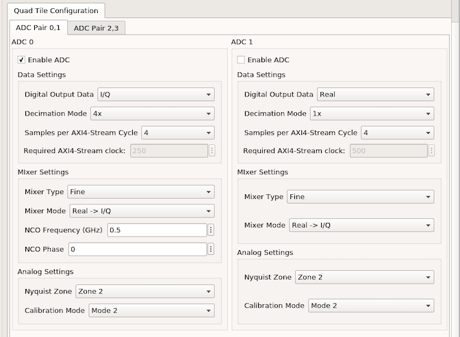
The next configuration section in the GUI configures the operation behavior of the ADCs within a tile. For a quad-tile platform configure this section as:
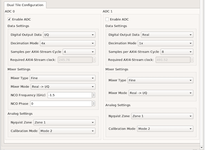
For a dual-tile platform configure this section as:
The selected configuration is not applied to all enabled tiles. While this does require some extra work, it allows for more flexibility in the design via changes in each individual tile. Even more flexibility is present in the ability to alter behavior within a tile as well, as long as they meet the same required AXI4-Stream clock requirement.
The Enable Tile checkbox under each ADC section enables the corresponding ADC. Under “Data Settings”,
Digital Output Data selects the output format of ADC samples where Real
bypasses the mixing signal path and I/Q will use the mixer and provide complex
basebanded samples. In this example we select I/Q as the output format using
the Fine mixer setting allowing for us to tune the NCO frequency. For more
information on the capabilities of both the coarse and fine mixer and NCO
examples see PG269 Ch.4, RF-ADC Mixer with Numerical Controlled
Oscillator.
The Decimation Mode drop down displays the available decimation rates that can
be applied for the generation platform targeted. Samples per AXI4-Stream Cycle
indicates how many 16-bit ADC words are output per clock cycle. The Required
AXI4-Stream clock field here displays the effective User IP clock that would be
required for the configuration of the decimator and number of samples per clock.
These fields are to match for all ADCs within a tile.
The Nyquist Zone setting selects either the first (odd, 0 <= f <= fs/2) or
second (even, fs/2 <= f <= fs) set of frequencies. In this example, for the quad-tile we target
Zone 2 with an NCO Frequency of 0.5 and the dual-tile has Zone 1 with an
NCO Frequency of -1.5.
With these configurations applied to the rfdc yellow block, both the quad-tile and
dual-tile platforms are outputting 4 adc words (64-bit) of complex basebanded I/Q data
centered at 1500 MHz. In the case of the quad-tile design with a sample rate of
2000 Msps and decimation of 4x, the effective bandwidth spans from 1250 to
1750 MHz. For the dual-tile design the effective bandwidth spans approx. from
1008.5 MHz to 1990.5 MHz.
Step 3: Update the platform yellow block
As mentioned above, when configuring the rfdc yellow block it reports the
required AXI4-Stream sample clock. This corresponds to the User IP Clk Rate of
the platform block. Typically, one would now update that field
to match what the rfdc reports, along with the RFPLL PL Clk
frequency that will be generating the clock used for the user design.
For this tutorial nothing should need to be done here, but in general this will need to be double-checked and aligned.
Step 4: Place and configure the Snapshot blocks
Next we capture the data the ADCs are producing using green
bitfield_snapshot block from the CASPER DSP Blockset library.
Add a bitfield_snapshot block to the design, found in CASPER DSP
Blockset->Scopes->bitfield_snapshot.

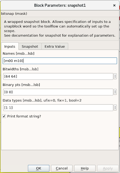
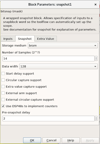
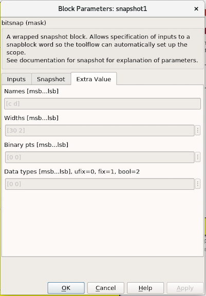
Configure the snapshot block as follows (note: for dual-tile platforms, the
name of the lsb should be m01 instead of m10):
Now hook up the bitfield_snapshot block to the rfdc block. In its current
configuration, the snapshot block takes two data inputs, a write enable, and a
trigger. Wire the first two dataoutput streams from the rfdc to the two in_*
ports of the snapshot block.
For the quad-tile platforms these are m00_axis_tdata and m10_axis_tdata. The
first digit in the signal name corresponds to the tile index — 0 for the first,
1 for the second, etc. The second digit in the signal name corresponds to the adc
index—in this case 0 is the first ADC input on each tile. In both Real and
I/Q digital output modes quad-tile platforms output all data bits on the same
bus. In this example, with 4 samples per clock this results in 2 complex
samples ordered {I1, Q1, I0, Q0}. As such, in each ADC word, the most recent
sample is at the MSB of the word. With the snapshot block configured to capture
2^14 128-bit words this is a total of 2^15 complex samples on both ports.
For dual-tile platforms in I/Q digital output modes, the inphase and
quadarature data are produced from different ports. In this mode the first digit
of the signal name corresponds to the tile index just as in the quad-tile.
Unlike in quad-tile, the second digit is 0 for inphase and 1 for
quadrature data. In this example then, with 4 samples per clock this is
4 complex samples with the two complex components coming from different
ports, m00_axis_tdata for inphase data ordered {I3, I2, I1, I0} and
m01_axis_tdata with quadrature data ordered {Q3, Q2, Q1, Q0}. When
configured in Real digital output mode the second digit is 0 for the
first ADC and 2 for the second. With the snapshot block configured to
capture 2^14 128-bit words this is a total of 2^16 complex samples
for the one port.
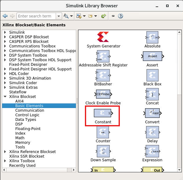
Next, leave write enable high, so add a blue Xilinx
constant block (Xilinx Blockset->Basic Elements->Constant), connect it to the
snapshot we port, and configure it as follows:
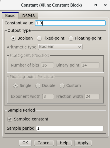
Using a blue Xilinx block instead of a white simulink block causes
the constant 1 to exist in the synthesized hardware design and
keep the write enable high.
Last, we want to be able to trigger the snapshot block on command in software.
To do this, we will use a yellow software_register and a green edge_detect
block (CASPER DSP Blockset->Misc->edge_detect).


Set the I/O direction of the software register to From Software, change the
Bitfield names to [start], and set Bitfield widths to 1 and Bitfield types
to 2. Connect this block’s output to the input of the edge detect block. Rename
the register to snapshot_ctrl (this will be the name for the register that is
visible in software—remember this name for later should you name it differently).
Finally, connect the output of the edge detect block to the trigger port on the snapshot
block. Now when we write a 1 to the software register, it will be converted
into a pulse to trigger the snapshot block.
Step 5: Validate the design
The design is now complete! For a quad-tile platform it should have turned out like this:
And like this for dual-tile platforms:
You can connect some simulink constant blocks to get rid of simulink unconnected
port warnings, or leave them if they do not bother you. Validate the design by
running the simulation. In this case, there’s nothing to see in the simulation,
but you can press ctrl+d to update and validate the diagram connections and
that port widths and data types are consistent. Make sure to save!
Step 6: Build!
As explained in tutorial 2, all you have to do to
build the design is run the jasper command in the MATLAB command window,
assuming your environment was set up correctly and you started MATLAB by using
the startsg command. The toolflow will take over from there and eventually
produce an .fpg file. When running this example, synthesis could take from 15-30 minutes,
depending on your build machine hardware.
As briefly explained in the first tutorial the toolflow will run one extra step that previous users may now notice. After Vivado synthesis and bitstream generation the toolflow exports the platform hardware definition to use Xilinx’s software tools (the Vitis flow) to generate software products to interface with the hardware design.
In this step the software platform hardware definition is read parsing the
design for IP with an associated software driver. This is done in two steps: the
hardware platform is ran first against Xilinx software tools and then a second
pass is taken augmenting those output products as neccessary with any CASPER-specific
additions. The result is any software drivers that interact with user
IP. In the case of the previous tutorial there was no IP with a corresponding
driver (other than the underlying Zynq processor); however, here we are using
the rfdc that has a fully configurable software component that we want to
communicate with in software. The resulting output at this step is the .dtbo
or device tree binary overlay which is a binary representation of the device
tree containing information for software drivers that is is applied at runtime
in software after the new bitstream is programmed.
Note: For the RFDC casperfpga object and corresponding software driver to
function correctly, this .dtbo must be created and when programming the board
must reside in the same level with the same name as the .fpg (but using the
.dtbo extension) when using casperfpga for programming.
Make sure then that the final bit of output of the toolflow build now reports
Created tut_rfdc-YYYY-MM-dd-hh-mm.dtbo.
Testing the Design
Before starting this segment, power-cycle the board. This is to force a hard
reset of the on-board RFPLL clocking network. After the board has rebooted,
start IPython and establish a connection to the board using casperfpga in the
normal way.
$ ipython
In [1]: import casperfpga

In [2]: zcu216 = casperfpga.CasperFpga('192.168.2.101')

In [3]: zcu216.upload_to_ram_and_program('/path/to/tut_rfdc.fpg')
This is our first design with the RFDC in it. When the RFDC is part of a CASPER
design the toolflow automatically includes meta information to indicate to
casperfpga that it should instantiate an RFDC object we can use to
manipulate and interact with the software driver components of the RFDC.
In [4]: zcu216.adcs
Out[4]: ['rfdc']
We can create a reference to that RFDC object and begin to exercise some of the software components included with that object.
In [5]: rfdc_zcu216 = zcu216.adcs['rfdc']
We first initialize the driver; a doc string is provided for all functions, letting one use IPythons help ? mechanism to get more information about a method’s signature and a brief description of its functionality.
In [6]: rfdc_zcu216.init?
Signature: rfdc.init(lmk_file=None, lmx_file=None, upload=False)
Docstring:
Initialize the rfdc driver, optionally program rfplls if file is present.

Args:
  lmk_file (string, optional): lmk tics hexdump (.txt) register file name
  lmx_file (string, optional): lmx tics hexdump (.txt) register file name
  upload (bool, optional): inidicate that the configuration files are local to the client and
    should be uploaded to the remote, will overwrite if exists on remote filesystem

Returns:
  True if completed successfully

Raises:
  KatcpRequestFail if KatcpTransport encounters an error
The init() method allows for optional programming of the on-board PLLs but, to
demonstrate some more of the casperfpga RFDC object functionality, run
init() without any arguments. This initializes the underlying software
driver with configuration parameters for future use.
In [7]: rfdc_zcu216.init()
Out[7]: True
We can then query the status of the rfdc using status().
In [8]: rfdc_zcu216.status()
ADC0: Enabled 1, State: 6 PLL: 0
ADC1: Enabled 1, State: 6 PLL: 0
ADC2: Enabled 1, State: 6 PLL: 0
ADC3: Enabled 1, State: 6 PLL: 0
Out[8]: True
The status() method displys the enabled ADCs, current “power-up sequence”
state information of the tile and the state of the tile PLL (locked, or not).
This information can be helpful as a first glance in debugging the RFDC should
the behavior not match the expected. The mapping of the State value to its
significance is found in Power-on Sequence Steps,
though in some cases the documentation is not very specific. In this case
6 indicates that the tile is waiting on a valid sample clock.
Note: RFSoC2x2 only provides a sample clock to tile 0 and 1 and, as it uses
a Gen 1 part that does not have the ability to forward sample clocks to other tiles,
1 and 3 for that platform will always halt at State: 6.
As the board was power-cycled before programming, any configuration of the
on-board PLLs was reset. To advance the power-on sequence state machine to
completion we need to program the PLLs. The RFDC object incorporates a few
helper methods to program the PLLs and manage the available register files:
progpll(), show_clk_files(), upload_clk_file(), del_clk_file().
First take a look at progpll():
In [9]: rfdc_zcu216.progpll?
Signature: rfdc.progpll(plltype, fpath=None, upload=False, port=None)
Docstring:
Program target RFPLL named by ``plltype`` with tics hexdump (.txt) register file named by
``fpath``. Optionally upload the register file to the remote

Args:
  plltype (string): options are 'lmk' or 'lmx'
  fpath (string, optional): local path to a tics hexdump register file, or the name of an
    available remote tics register file, default is that tcpboprphserver will look for a file
    called ``rfpll.txt``
  upload (bool): inidicate that the configuration file is local to the client and
    should be uploaded to the remote, this will overwrite any clock file on the remote
    by the same name
  port (int, optional): port to use for upload, default to ``None`` using a random port.

Returns:
  True if completes successfuly

Raises:
  KatcpRequestFail if KatcpTransport encounters an error
To program a PLL we provide the target PLL type and the name of the
configuration file to use. Optionally, we can upload a file for later use. With
upload set to False this indicates that the target file already exists on the
remote processor for PLL programming. As the current CASPER supported RFSoC
platforms use various TI LMX/LMK chips as part of the RFPLL clocking
infrastructure, the progpll() method is able to parse any hexdump export of a
TI TICS Pro file (the .txt formatted file).
show_clk_files() will return a list of the available clock files that are
available for reuse; the distributed CASPER image for each platform provides the
clock files needed for this tutorial. We use those clock files with progpll()
to initialize the sample clock and finish the RFDC power-on sequence state
machine. Follow the code relevant for your selected target (make sure to have
reviewed your platforms [page](./readme.md#platforms) for any required setup):
# clock files for different platforms

# ZCU216
In [10]: c = rfdc_zcu216.show_clk_files()

In [11]: c
Out[11]: ['250M_PL_125M_SYSREF_10M.txt']

In [12]: rfdc_zcu216.progpll('lmk', c[0])
Out[12]: True

# ZCU111
In [13]: c = rfdc_zcu111.show_clk_files()

In [14]: c
Out[14]: ['122M88_PL_122M88_SYSREF_7M68_clk5_12M8.txt',
'LMX_REF_122M88_OUT_245M76.txt']

In [15]: rfdc_zcu111.progpll('lmk', c[0])
Out[15]: True

In [16]: rfdc_zcu111.progpll('lmx', c[1])
Out[16]: True

# RFSoC 4x2
In [17]: c = rfdc_rfsoc4x2.show_clk_files()

In [18]: c
Out[18]: ['rfsoc4x2_LMX_REF_245M76_OUT_491M52.txt',
'rfsoc4x2_PL_122M88_REF_245M76.txt']

In [19]: rfdc_rfsoc4x2.progpll('lmk', c[1])
Out[19]: True

In [20]: rfdc_rfsoc4x2.progpll('lmx', c[0])
Out[20]: True

# RFSoC 2x2
In [21]: c = rfdc_2x2.show_clk_files()

In [22]: c

Out[22]: ['rfsoc2x2_lmk04832_12M288_PL_15M36_OUT_122M88.txt',
'LMX_REF_122M88_OUT_245M76.txt']

In [23]: rfdc_2x2.progpll('lmk', c[0])
Out[23]: True

In [24]: rfdc_2x2.progpll('lmx', c[1])
Out[24]: True

# ZRF16
In [25]: c = rfdc_zrf16.show_clk_files()

In [26]: c
Out[26]: ['rfsoc2x2_lmk04832_12M288_PL_15M36_OUT_122M88.txt',
'zrf16_LMX_REF_50M_OUT_250M.txt']

In [27]: rfdc_zrf16.progpll('lmk', c[0])
Out[27]: True

In [28]: rfdc_zrf16.progpll('lmx', c[1])
Out[28]: True
With the clocks programmed we can now check the status of the rfdc and it
should now report that the tiles have locked their internal PLLs and have
completed the power-on sequence by displaying a state value of 15.
In [25]: rfdc_zcu216.status()
ADC0: Enabled 1, State: 15 PLL: 1
ADC1: Enabled 1, State: 15 PLL: 1
ADC2: Enabled 1, State: 15 PLL: 1
ADC3: Enabled 1, State: 15 PLL: 1
Out[25]: True
The remaning methods, upload_clk_file() and del_clk_file() are available
methods used to manage the clock files available for programming.
The ADC is now sampling and we can begin to interface with our design to copy back samples from the BRAM and take a look at them. The following are a few helper methods that can be used for this example.
def toSigned(v, bits):
  mask = 1 << (bits-1)
  return -(v & mask) | (v & (mask-1))

def capture_snapshots(fpga):
  snapshot_data = {}
  for ss in fpga.snapshots:
    ss.arm()

  fpga.registers.snapshot_ctrl.write(start='pulse')
  for ss in fpga.snapshots:
    dat = ss.read(arm=False)['data']

    for (k,v) in dat.items():
      snapshot_data[k] = v

  return snapshot_data

def deinterleave_dual(I, Q, bits=16):
  x = []
  for (i, q) in zip(I, Q):
    I0 = toSigned(0xffff & (i >> 0) , bits)
    I1 = toSigned(0xffff & (i >> 16), bits)
    I2 = toSigned(0xffff & (i >> 32), bits)
    I3 = toSigned(0xffff & (i >> 48), bits)

    Q0 = toSigned(0xffff & (q >> 0) , bits)
    Q1 = toSigned(0xffff & (q >> 16), bits)
    Q2 = toSigned(0xffff & (q >> 32), bits)
    Q3 = toSigned(0xffff & (q >> 48), bits)

    x0 = I0 + 1j*Q0
    x1 = I1 + 1j*Q1
    x2 = I2 + 1j*Q2
    x3 = I3 + 1j*Q3

    x.append(x0)
    x.append(x1)
    x.append(x2)
    x.append(x3)

  return x

def deinterleave_quad(samples, bits=16):
  x = []
  for s in samples:
    I0 = toSigned(0xffff & (s >> 0) , bits)
    Q0 = toSigned(0xffff & (s >> 16), bits)
    I1 = toSigned(0xffff & (s >> 32), bits)
    Q1 = toSigned(0xffff & (s >> 48), bits)

    x0 = I0 + 1j*Q0
    x1 = I1 + 1j*Q1

    x.append(x0)
    x.append(x1)

  return x
The capture_snapshot() method helps extract data from the snapshot block by
iterating over the snapshot blocks in this design (only one right now) and
arming them to look for a pulse event and then toggles the software register
snapshot_ctrl to trigger the capture event. If in the design process this
software register name is different than shown here, you will need to
updated this in this method. Same with the bitfield name of the software register.
Here it was called start when configuring the software register yellow block.
Using these methods to capture data for a quad- or dual-tile platform and then
plotting the first few time samples for the real part of the signal would look
something like the following (make sure to replace the fpga variable with your
casperfpga object instance):
import numpy as np
import matplotlib.pyplot as plt

# quad-tile
def qt_capture(fpga):
  adc_dat = capture_snapshots(fpga)
  m00 = adc_dat['m00']
  m10 = adc_dat['m10']
  x_m00 = np.array(deinterleave_quad(m00, 16))
  x_m10 = np.array(deinterleave_quad(m10, 16))
  return (x_m00, x_m10)

N = 100
n = np.arange(0,N)
x_m00, x_m10 = qt_capture(fpga)
fig, ax = plt.subplots(2,1, sharey='row')
ax[0].plot(n, np.real(x_m00[0:N])); ax[0].set_title('Tile 0 Ch.0'); ax[0].grid(True);
ax[1].plot(n, np.real(x_m10[0:N])); ax[1].set_title('Tile 1 Ch.0'); ax[1].grid(True); plt.show();

# dual-tile
def dt_capture(fpga):
  adc_dat = capture_snapshots(fpga)
  I = adc_dat['m00']
  Q = adc_dat['m01']
  x = np.array(deinterleave_dual(I, Q, 16))
  return x

N = 100
n = np.arange(0, N)
x = dt_capture(fpga)
plt.plot(np.real(x[0:N])); plt.title('Tile 0 Ch.0'); plt.grid(); plt.show();
Output of dualtile test with 1.450 GHz input:

Conclusion
In this tutorial it was shown how to configure and use the rfdc yellow block
for both dual- and quad-tile RFSoC platforms. An example design was built for
both architectures sampling an RF signal centered in a band at 1500 MHz. It was
shown how to use casperfpga to access the RFDC object, initialize the
driver, and use some of the methods provided to program the onboard PLLs. The
example design allowed us to capture samples into a BRAM and read those back
into software for more analysis.