GPIO
gpio)Contents |
Summary
The gpio block provides access to GPIO pins on any board that has GPIO headers.
Mask Parameters
Parameter |
Variable |
Description |
|---|---|---|
I/O group |
io_group |
Selects the board architecture and the GPIO header on that board. |
I/O direction |
io_dir |
Chooses whether the pin sends data |
Data Type |
arith_type |
Specifies data type of register. |
Data bitwidth |
bitwidth |
Specifies data bitwidth. |
Data binary point |
bin_pt |
Specifies the binary point position of data. |
GPIO bit index |
bit_index |
Specifies the pin on the selected GPIO header. |
Sample period |
sample_period |
Specifies sample period of interface. |
Use DDR |
use_ddr |
??? |
Pack register in the pad |
reg_iob |
??? |
Register clock phase |
reg_clk_phase |
|
Termination method |
termination |
|
Ports
Port |
Dir |
Data Type |
Description |
|---|---|---|---|
reg_out |
in |
inherited |
Output from design to GPIO pin. Only in I/O |
sim_out |
out |
double |
Simulation output of pin value. Only in I/O |
sim_in |
in |
double |
Simulation input of pin value. Only in I/O |
reg_in |
out |
inherited |
Input from GPIO pin to design. Only in I/O |
Description
ROACH Specific Information
Main article: ROACH FPGA Interfaces
Each GPIO header has one direction selector that controls the direction
of all 8 of its pins. You must set a direction. So, in addition to your
normal gpio block (configured for I/O group ROACH:gpio[ab]), add
another gpio block, and set the following parameters:
I/O group =
ROACH:gpio[ab]_oe_nI/O direction =
outbitwidth =
1bit_index =
0
The direction selector takes a boolean value as its input, so wire it to a Xilinx constant block:
0- output from ROACH1- input to ROACH
The two SMA connectors on the back of the board are wired directly to GPIO pins. Specifically, J11 and J10 are wired to pins 6 and 7 on GPIO A.
Notes
The order of the FPGA GPIOs have been changed from “3 2 1 0 7 6 5 4” to now match the order printed on the PCB “0 1 2 3 4 5 6 7”.
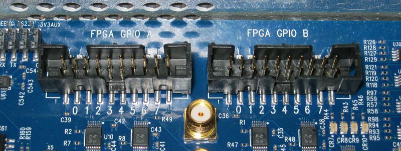
Old mapping: 3 2 1 0 7 6 5 4
New mapping: 0 1 2 3 4 5 6 7